Los Pinos
| Complejo Cultural de Los Pinos | |
|---|---|
 The Casa Miguel Alemán | |
 | |
| General information | |
| Architectural style | Neoclassical Eclectic |
| Address | Casa Miguel Alemán, PB, Col. San Miguel Chapultepec, 11850, Mexico City |
| Coordinates | 19°24′56″N 99°11′29″W / 19.41556°N 99.19139°W |
| Technical details | |
| Structural system | Casa Miguel Alemán Casa Lázaro Cardenas Casa Anexa Jardines Plaza Francisco I. Madero Calzada de la Democracia Molino del Rey |
| Design and construction | |
| Architect(s) | Multiple Manuel Giraud Esteva designed the Casa Miguel Alemán |
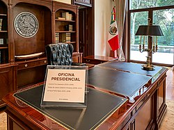
Los Pinos (English: The Pines) was the official residence and office of the President of Mexico from 1934 to 2018. Located in the Bosque de Chapultepec (Chapultepec Forest) in central Mexico City, it became the presidential seat in 1934, when Gen. Lázaro Cárdenas became the first president to live there. The term Los Pinos became a metonym for the Presidency of Mexico.
Since December 2018, the former presidential complex has operated as a cultural space.
History
[edit]
After the Spanish Conquest, around 1550, a trapiche (mill) was built in Chapultepec, where wheat and maize were processed into flour.[1] This mill became so important that it was later called the Molino del Rey ("The King's Mill").[1]
In 1853, the Molino del Rey was sold to Doctor José Pablo Martínez del Río, who built the Casa Grande ("Grand House") that would later become known as Rancho La Hormiga ("The Ant Ranch"). In 1865, the whole property was sold to Emperor Maximilian for a total of 25,000 Mexican pesos. Following the 1867 overthrow and execution of Maximilian, the property was, in 1872, returned to Doctor Martínez del Río.[2]
Government residence
[edit]In 1917, with the end of the armed phase of the Mexican Revolution, President Venustiano Carranza expropriated the properties. So that his most trustworthy cabinet member could live there, he paid N$886,473 for both the property and the construction of a residence that would be close to Chapultepec Castle, which at the time was used as the official residence. Because of this, the first inhabitant of the residence was Álvaro Obregón, while he held the post of Navy and War Secretary.[1] After his tenure, the residence was unused.
In 1934, President Lázaro Cárdenas took office but refused to use the Castle of Chapultepec as his official residence, as he thought it too ostentatious. He was offered use of Rancho la Hormiga (The Ant Ranch), which he accepted. He changed its name to Los Pinos (The Pines) for two reasons: first, he did not consider the name La Hormiga to be accordant with the residence of a President and, second, he promised his wife that when he became president, the house they shared would be named after the huerta in Tacámbaro, Michoacan, where they met.[1]
Los Pinos was home to thirteen of the fourteen presidents in office between 1935 and 2018, with the exception of Adolfo López Mateos (1958–1964).[3] In 2000, President Vicente Fox chose one of the nearby cottages as his home and the Casa Miguel Alemán (residence of most prior presidents) was used for offices and other government functions.
Cultural space
[edit]
In 2018, Andrés Manuel López Obrador, at the time a candidate for the Mexican presidency, announced that he would not live in Los Pinos if he won the election and would instead open the residence to the public.[4] López Obrador won the election, and Los Pinos was opened to the public on December 1, 2018, the day of López Obrador's presidential inauguration. López Obrador moved the presidential offices back to the National Palace where he lived for the entirety of his presidency.[5]
In 2020 during the COVID-19 pandemic in Mexico, doctors and nurses were housed at the complex.[6]
Since taking office on October 1 of 2024, President Claudia Sheinbaum has resided in the National Palace keeping Los Pinos open to the public.
References
[edit]- ^ a b c d "Los Pinos: historia de la casa del próximo Presidente de México". Animal Politico. 23 July 2012. Retrieved 17 October 2015.
- ^ "La historia de Los Pinos". El Universal. Retrieved 17 October 2015.
- ^ Becerril, Andrés (11 November 2018). "Los Pinos, el poder como inquilino; se acerca el fin de una era". Excélsior (in Spanish). Retrieved 11 November 2018.
- ^ Partlow, Joshua (4 June 2018). "If he becomes president, this man will turn Mexico's White House into a public park". Washington Post. Retrieved 1 December 2018.
- ^ Sieff, Kevin (1 December 2018). "Mexico's president has turned the presidential mansion into a museum". Washington Post. Retrieved 1 December 2018.
- ^ "Mexico turns ex-presidential residence into coronavirus base for nurses, doctors". Reuters. 8 May 2020. Retrieved 6 February 2021.
External links
[edit]- Presidencia de la República website (in Spanish)


